
The BEE3 (Berkeley Emulation Engine, version 3) is a multi-FPGA system with up to 64 GB of DRAM and several I/O subsystems that can be used to enable faster, larger and higher fidelity computer architecture or other systems research.
Objective: Revitalizing Computer Architecture Research
The Problem
- Computer Architecture is increasingly incremental, and boring.
- Many papers study a tiny feature, and report 5% improvements.
- Simulation is too slow to allow full-system experiments running real software.
- Researchers can no longer build real chips to test new ideas – it’s too expensive.
Our Goal: Change this
- Provide an experimental platform for the research community.
The Solution: BEE3
BEE3 stands for the Berkeley Emulation Engine version 3. The BEE3 system is a 2U chassis with a tightly-couple 4 FPGA system that is a vehicle for Computer Architecture Research. In particular, the BEE3 is the target platform for the Research Accelerator for Multiple Processors (RAMP). RAMP is a collection of six universities (Berkeley, Stanford, UW, UT, CMU, and MIT) and several industry partners including: Microsoft Research, Xilinx, Sun Microsystems and IBM. The BEE3 is a scalable platform, 1 to 64 2U systems, that facilitates research in a multiple areas: Computer Architecture, Systems, OS and Software, Memory Hierarchy and Storage, and various Application/Algorithm Accelerators, to name a few.
-
The BEE3 design has been licensed to BEEcube. Please contact BEEcube for product ordering and pricing information.
The BEE3 DDR2 controller is available at the Microsoft Research downloads repository. You can also search for the controller by name: “DDR2 DRAM Controller for BEE3”.
The pictures below show the rack mounted 2U BEE3 system and the inside of the 2U system with the major components labeled.

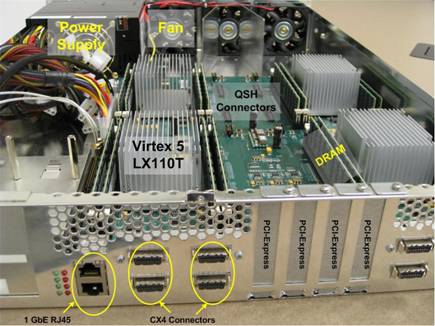
The BEE3 system is made up of a Main Printed Circuit Board (PCB) and a Control & I/O PCB with the following components:
- 2U Enclosure with standard PC components
- Fans, power supply, etc.
- BEE3 Main PCB
- 4 Xilinx FPGAs (FF1136 package)
- Virtex-5 LX110T, LX155T, or SX95T
- 16 DDR2 DIMMs
- 2 DDR2 (400) channels per FPGA
- Up to two 4 GB DIMMs per channel
- FPGA Ring Interconnect
- 8 10 GBase-CX4 Interfaces
- 4 PCI-Express slots (endpoint only)
- 4 QSH-DP (40 LVDS pairs) Connectors
- 4 1GbE RJ45 Ports
- BEE3 Control & I/O PCB
- 4 RS232 via RJ45 Connectors
- 4 SD Slots
- Per FPGA Persistent Storage
- 1 Compact Flash slot and System Ace support
- FPGA Configuration Storage (Bit Files)
- 1 Xilinx USB-JTAG Interface
- 2 SMA Clock Inputs
- Power Switch
- Global Reset Button
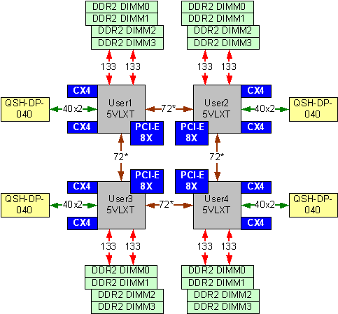
The BEE3 Main PCB connectivity is shown in the diagram below:
- 2U Enclosure with standard PC components
-
People
Chuck Thacker
Emeritus Researcher