Chapter 45
The TI ASC: A Highly Modular and Flexible Super Computer Architecture1
W. J. Watson
Introduction
Early in 1966, a large computer development program was begun by Texas Instruments. The goal for this effort was to provide needed capacity for supporting seismic processing, plus offering a general super computer capability in the support of new markets.
This development has resulted in the Advanced Scientific Computer (ASC)¾
a highly modular system offering a wide spectrum of computing power and
configurability.
Overview of the System
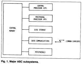
The major subsystems of a typical configuration are shown in Fig. 1: the central memory, the central processor, the peripheral processor, on-line bulk storage, a digital communications interface, plus a selection of standard peripherals.
The peripheral processor has been designed for executing the operating
system. The central processor has been designed expressly to provide high
computing power for large arrays of data. The central processor operates
as a slave to the peripheral processor. This design approach was chosen
to maximize the overlapping of system overhead tasks with the execution
of user programs. In operation the job stream is analyzed by the peripheral
processor. The language processors, plus user object code, are executed
by the central processor. System control and I/O tasks are processed
by the peripheral processor. I/O is routed through high-speed, head-per-track
disc storage. A data communications interface for the common carriers is
provided for the support of remote hatch and interactive terminals. Standard
types of peripherals are also provided. The central memory serves as the
common access communications and access storage medium for these subsystems.
Central Memory
The ASC central memory consists of a memory control unit (MCU) and appropriately sized modules of high-speed or
medium-speed central memory. Optionally, a medium-speed central memory extension can be used in conjunction with a high-speed memory.
The MCU is organized as a two-way, 256-bit/channel (8-word) parallel access traffic net between eight independent processor ports having full accessibility to all memories. The nine memory buses are organized to provide eight-way interleaving for the first eight buses with the ninth bus used for the central memory extension. The MCU provides the facilities for controlling access from the eight processor ports to a CM having a 24-bit address space (16 million words). A port expander can be utilized to expand the number of processor ports. Fig. 2 illustrates this structure.
The MCU is designed to operate asynchronously, independent of cable delays, processor clock rates, and memory unit access and cycle times. This capability allows for a great deal of flexibility to accommodate improvements in memory or processor technologies which may be desired. The MCU is capable of handling a maximum data transfer rate of 80 million words per second per port, giving a total transfer capacity of 640M words per second. Therefore, a significant capacity beyond today's memory and processor speeds is available in the MCU.
The semiconductor high-speed central memory modules have a cycle time of 160 ns and a read time of 140 ns. Additionally, all transfers are 256 bits (eight 32-bit words) with a Hamming code providing single-bit error correction and double-bit error detection for each 32-bit word. High-speed central memory is typically divided into eight equal sized modules which permits eight-way interleaving. A patch board within the MCU controls the memory address decoding and sets the interleaving pattern.
The optional central memory extension provides for large
1Proc. AFIPS FICC, 1972, pp. 221-228. The section on software beginning on p. 759 is excerpted from Dean [1973].