Chapter 8½ Structural Levels of
the PDP-8 111
conveniently represents the constitutent objects of each level and their
interconnection at the next highest level.
The PMS Level
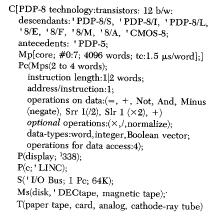
The PDP - 8 computer in PMS notation is:
As an example of PMS structure, the LINC-8-338 is shown in Fig. 2; it consists of three processors (designated P): Pc(' LINC), Pc(' PDP-8), and P.display( '338). The LINC processor is a very capable processor with more instructions than the PDP-8 and is available in the structure to interpret programs written for the LING. Because of the rather limited instruction set being interpreted, one would hardly expect to find all the components present in Fig. 2 in an actual configuration.
The switches (S) between the memory and the processor allow eight primary memories (Mp) to be connected. This switch, in PMS called S(' memory Bus; 8 Mp; 1 Pc; time-multiplexed; 1.5 m s/word), is actually a bus with a transfer rate of 1.5 microseconds per word. The switch makes the eight memory modules logically equivalent to a single 32,768-word memory module. There are two other connections (a switch and a link) to the processor excluding the console. They are the S(' I/O Bus) and L(' Data Break; Direct Memory Access) for interconnection with peripheral devices. Associated with each device is a switch, and the I/O Bus links all the devices. A simplified PMS diagram (Fig. 3) shows the structure and the logical-physical transformation for the I/O Bus, Memory Bus, and Direct Memory Access link. Thus, the I/O Bus is:
![]()
The I/O Bus is nearly the same for the PDP-5, 8, 8/S, 8/I, and 8/L. Hence, any controller can be used on any of the above computers provided there is an appropriate logic level converter (PDP-5, 8, and 8/S use negative polarity logic; the 8/I and 8/L, positive logic). The I/O Bus is the link to the controllers for processor-controlled data transfers. Each word transferred is designated by a processor in-out transfer (IOT) instruction. Due to the high cost of hardware in 1965, the PDP-8 I/O Bus protocol was designed to minimize the amount of hardware to interface a peripheral device. As a result, only a minimal number of control signals were defined with the largest portion of I/O control performed by software.
A detailed structure of the processor and memory (Fig. 4) shows the I/O Bus and Data Break connections to the registers and control in the notation used in the initial PDP-8 reference manual. This diagram is essentially a functional block diagram. The corresponding logic for a controller is given in Fig. 3 in terms of logic design elements (ANDs and ORs). The operation of the I/O Bus starts when the processor sends a control signal and sets the six I/O selection lines (IO. SELECT <0:5>) to specify a particular controller. Each controller is hardwired to respond to its unique 6-bit code. The local control, K[k], select signal is then used to form three local commands when ANDed with the three IOT command lines from the processor. These command lines are called IO. PULSE, 1, IO. PULSE. 2, and IO. PULSE.4. Twelve data bits are transmitted either to or from the processor, indirectly under the controller's control. This is accomplished by using the AND/OR gates in the controller for data input to the processor, and the AND gate for data input to the controller. A single skip input is used so that the processor can test a status bit in the controller. A controller communicates back to the processor via the interrupt request line. Any controller wanting attention simply ORs its request signal into the interrupt request signal. Normally, the controller signal causing an interrupt is also connected to the skip input, and skip instructions are used in the software polling that determines the specific interrupting device.
The Data Break input for Direct Memory Access provides a direct access
path for a processor or a controller to memory via the processor. The number
of access ports to memory can be expanded to eight by using the DM01 Data
Multiplexer, a switch. The DM01 port is requested from a processor (e.g.,
LINC or Model 338 Display Processor) or a controller (e.g.', magnetic tape).
A processor or controller supplies a memory address, a read or write access
request, and then accepts or supplies data for the accessed word. In the
configuration (Fig. 1), Pc[' LINC] and P[ '338] are connected to the multiplexer
and make requests to memory for both their instructions and data in the
same way as the PDP-8 processor. The global control of these processor
programs is via the processor over the I/O Bus. The processor issues start
and stop commands, initializes their state, and examines their