Chapter 6 ½ Structure 63
the circuit level and from pressure above, requiring the memories to be developed. All the electromechanical secondary memories (e.g. magnetic tape, drums, disks, and photostores) have resulted from the computer's needs. Special packaging (e.g., the dual inline package, or DIP) and interconnect (e.g., printed circuit boards, chip carriers) technologies were also developed for computers. Thus, despite the dominant technology, the computer often shapes development.
The transistor and integrated circuit have had a profound impact on the structure of computers. Further, the proliferation of computer structures built from these technologies has provided enough data points that several interesting trends can be seen.
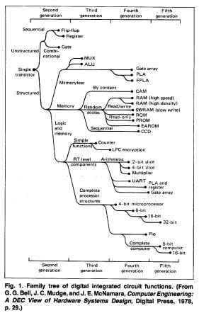
Figure 1 shows a family tree (taxonomy) of the most common digital integrated circuits.1 The least complex functions are in the upper portion of the figure, and the most complex are at the bottom. In addition, the circuits are ordered by generation, starting with the second generation on the left side of the figure and progressing to the fifth generation on the right side. The circuits are clustered roughly by the regularity of the function and whether memory is associated with the function. Circuit regularity is important in large-scale integrated circuits because it is desirable to implement regular structures to minimize area-consuming interconnections and, thus, to simplify layout and understanding and to aid testing.
As indicated in Fig. 1, the branching of the integrated circuit family tree began in earnest at the beginning of the third generation. At that time, advances in integrated-circuit technology permitted collections of basic logic primitives (AND, NAND, etc.) and sequential circuit components (flip-flops, registers, etc.) to occupy a single integrated circuit rather than an entire module. This had the benefit of providing a drastic reduction in size between the second and third generation computer designs. But it also had the drawback that modules contained a wide variety of functions and were thus specialized.
As the densities began to approach 100 gates, the construction of complete arithmetic units on a single chip became possible. The earliest and most famous chip, the 74181 arithmetic logic unit (ALU), provided up to 32 functions of two 4-bit variables. By the fourth generation, it became possible to construct on a single chip very large combinational circuits, such as a complete 16- by 16-bit multiplication circuit (e.g., the TRW Corp. multiplier) requiring about 5,000 gates.
Progress during the fourth and fifth generations has not been without its problems, however. Without well defined functions such as addition and multiplication, semiconductor suppliers
cannot provide high density products in high volume because there are few large-scale, general purpose universal functions.
To address these problems, two methods of effectively customizing large-scale
integrated circuit logic are included in Fig. 1. These are the programmable
logic array (PLA) and the gate array (also called master slice.) The programmable
logic array (PLA) is an array of AND-OR gates that can be interconnected
to form the sum-of-products terms in a combinational logic design. Gate
arrays are simply a large number of gates placed on the chip in
1Figure 1 and the discussion surrounding it are adapted
from Bell, Mudge, and McNamara [1978].