452 EVOLUTION OF COMPUTER BUILDING BLOCKS
Control Part
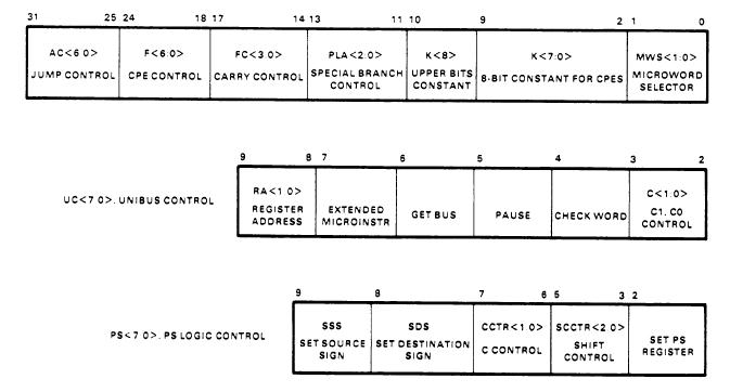
The Control part of the CMU-l1 uses the Microprogram Control Unit and a 512-word control store* with 32-bit microinstructions. Figure 4 shows the format of the microinstruction and Table 1 briefly describes the function of each of the fields. A microinstruction buffer register was included in the design to allow the overlap of the fetch of the next microinstruction with the execution of the current microinstruction, which is a common technique to improve the performance of microprogrammed processors.
The "next-address logic" of the 3001 has been augmented by additional microbranch control logic external to the 3001. This external logic uses the contents of the instruction register, the condition codes in the PS, and the PLA field from the microinstruction register to determine the AC<6:0> lines to input to the 3001.
Figure 4. Microinstruction format.
The other major section of control logic that had to be added to the design was the processor status logic to control the setting of the 4-bit condition code in the PS register and control access to the PS. In fact, the PS register is defined as primary memory location 177776 in the PDP-11 architecture and requires special logic to load and store the PS.
Interface to the Unibus
A significant fraction of the components of the CMU-l1 are devoted to the support of the Unibus. Given the demanding electrical requirements of the Unibus, the tri-state A, D, and M lines of the 3002 array could not be directly attached to the Unibus. Instead, separate transceiver packages had to be used to provide this buffering.
Due to the asynchronous operation of the Unibus and interrupt and nonprocessor
___________________
* In order to expedite the debugging of the microprogram for the CMU-l1, we built a fast, simple writable control store for the CMU. We used 45-nanosecond access time, 1024-bit random-access memory (RAM) packages to ensure a writable control store as fast as the final read-only memory (ROM) control store. The writable control store is interfaced to a Unibus (of a PDP-1 1 other than the CMU-11) for initial loading of microprograms. Figure 3 shows the CMU-l I interfaced to the supporting PDP-l 1 and writable control store.